Sand Wafers Chips and Beyond – the Intel Experience

Silicon a natural semiconductor and the most abundant material on earth after oxygen is the backbone of the microprocessor industry. Found plentifully on beach sand, it has to be melted, purified and cooled to form an ingot. The almost hundred percent pure (99.999) silicon ingot is then sliced into discs called wafers. Chips are then built on the wafer surface in a fabrication facility called “fab”. Making chip is a very complex process requiring maybe up to fifteen hundred independent operations. The engineering depending on the chip's intended use. Chips look flat to the naked eye but in reality are three dimensional structures and may include dozens of layers of complex circuitry. Necessity is the mother of inventionthey say and the necessity for more efficient, powerful and less expensive chip is the driving force behind their technological development.
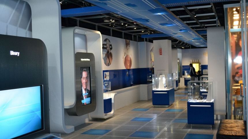
The Intel Museum located in Robert Noyce Building of the Intel Headquarters in Santa Clara, California has exhibits of Intel products and depicts its proud history. The museum started in 1980 and opened to public viewing twelve years later. Admission to the museum is free and open Monday through Saturday. Located in the hub of Silicon Valley the 10,000 sq ft museum offers a rare insight into the high tech industry of the world's largest chip manufacturer. It contains iterative displays of how silicon chips are made, how they work and above all how they power our digital world. The self- guided tour of the museum was an experience that we shall never forget. With dozens of exhibits the museum also chronicles the life of its innovative genius Robert Noyce (1927-1990) – Intel's co-founder and the co-inventor of the integrated circuit or microchip (along with Jack Kilby). The realization of microchip that powered the personal computer revolution is believed to be the reason behind Silicon Valley's name and Robert Noyce is lovingly called the “Mayor of Silicon Valley”. The Intel timeline also sketches the life of another co-founder Gordon Moore (1929 - ). Moore is credited with the observation that transistors the basic building block of microchips will both decrease in size and cost at an exponential rate. For more than fifty years since 1965, his prediction has led to more efficient and powerful microchip that powered personal computer, tablets, smart phones, data collection, retrieving and transmitting centers etc. The observation now known as Moore's Law says “The number of transistors incorporated in a chip will approximately double in every 24 months”.
The purest thing we will ever touch – a silicon ingot is also on display. Subsequently the silicon chip manufacturing processes are shown in the Intel Fab exhibit area over close circuit TV, where scientists and technicians in “bunny suits” in ultra clean environment work through the complex processes. We also simulated the Fab conditions in the museum by putting on bunny suits and walked around the perforated flooring through which purified air 100 times cleaner than a hospital operating theater circulates. Another interesting display allows us to “spell” our name in two digit binary language computer. Intel's first microprocessor 4004 and the evolution to its present state where more than a billion transistors are stacked in a wafer the size of a finger nail are also on display. The most sophisticated processor containing billions of transistors are interconnected by fine copper wire that controls the flow of electricity through the chip to send, receive and process information. Time has thus to be measured in billionth of a second and distances to billionth of a meter. The original IBM PC containing the Intel 8088 microprocessor is also on display.
Intel's manufacturing and fabrication facilities “fabs”, in and around Hillsboro, Oregon spreads over four huge campuses. These campuses comprise Intel's largest and most sophisticated sites in the world. The company has over 17,000 employs in Oregon making it the state's largest private investor. With the addition of two new facilities MOD1 and MOD2 at the Ronler Acers Campus, Hillsboro, the company's research and fabrication facilities are poised to break new grounds in semi-conductor technology. It is a great feeling to find that at these facilities more than two hundred engineers from Bangladesh are actively engaged in research and manufacturing. Apart from Intel there are smaller industries in and around the area that has earned it the nickname “Silicon Jungle”
In the last interview Noyce was asked by journalists what he would do if he were “Emperor of USA”. He replied he would among other things “make sure we are preparing our next generation to flourish in a high – tech age. And that means education of the lowest and poorest, as well as at the graduate school level”.
The writer is Professor of Physics, Jahangirnagar University,
Fellow of the Royal Astronomical Society (UK),
Fellow of the Bangladesh Physical Society and
Currently visiting Hillsboro, Oregon, USA.

 For all latest news, follow The Daily Star's Google News channel.


Comments