Bangladesh can become a semiconductor packaging hub

Recently, there have been discussions going on in the country on developing a semiconductor manufacturing sector, in an effort to diversify our economy and accelerate economic growth. Semiconductor chips, or integrated circuit (IC) chips, are the brains of modern electronic devices. In 2020, more than 932 billion chips were produced in the world – that's more than 116 chips per person. You may be using more than 150 IC chips on a daily basis via your smartphone, depending on the model. In the era of Fourth Industrial Revolution (4IR), the demand for IC chips is only going to rise, which means semiconductor manufacturing will keep growing; the semiconductor market is expected to almost double in value, to become a USD 1 trillion industry, by the end of this decade.
Manufacturing IC chips and integrating them into commercial electronic devices constitute probably the most technologically advanced and complex manufacturing value chain. Simply put, the major steps in semiconductor manufacturing include: 1) IC chip design; 2) silicon wafer production; 3) IC chip fabrication; 4) IC chip packaging, assembly and testing; and 5) integration to systems/commercial products.
In Bangladesh, some IC design-related activities have started recently. But that is not the focus of this article. Out of the steps listed above, IC chip fabrication, also called front-end process, consists of highly sophisticated process steps that need huge capital (several billion US dollars), highly skilled engineers and scientists, and intense involvement in advanced research and development (R&D). Only a few companies in the world are able to do IC fabrication, such as TSMC, Intel, Samsung, Global Foundries, etc. At present, it is not realistic for Bangladesh to enter the IC chip fabrication sector. But what is doable right now is IC chip packaging, assembly and testing.
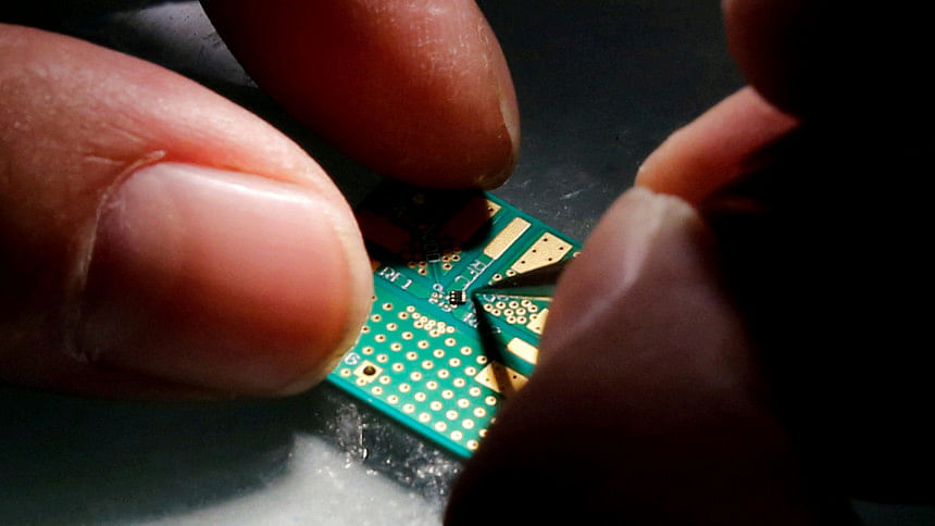
For simplicity, let's use "packaging" to refer to this step, which is also called back-end process. An IC chip, built on a thin single crystal silicon wafer, is vulnerable, fragile, and easily gets damaged when exposed to the ambient atmosphere. So, it must be secured in a package that provides the necessary protection against mechanical, thermal, and chemical damages. An IC chip cannot work on its own. Hence, the package must provide connection between the chip and other circuit components. The package must also dissipate the heat generated because of the current flowing through the chip so as not to overheat and destroy it.
An IC package is a highly complex engineered product that needs multidisciplinary science and engineering expertise to design and manufacture. A lot of value addition happens in this segment of semiconductor manufacturing. Forecast by Straits Research, a leading market research organisation, shows that Outsourced Semiconductor Assembly and Test (OSAT) services are growing at a compound annual growth rate of 8.5 percent, from $37.95 billion in 2021 to an estimated $72.90 billion in 2030.
IC packaging is technologically less demanding and labour-intensive. That is why this segment of semiconductor manufacturing was shifted from the West to the Asia-Pacific region in the early 1980s. Packaging has been thriving in this region that used to offer low wages – e.g. in Malaysia, China, Taiwan, etc. However, labour costs in these countries have risen over the years. IC packaging is again being shifted to new, lower-wage countries. Vietnam, taking advantage of this shift, has been able to attract multi-billion-dollar foreign direct investment (FDI) in semiconductor manufacturing. Companies like Intel, Samsung, LG, AmKor, Panasonic, Foxconn, etc have been investing heavily in high-tech parks in Vietnam. The Philippines is also reaping benefits from this trend. India, too, has entered the semiconductor industry very recently in an emphatic way.
Against this backdrop, Bangladesh can position itself to be an active player, particularly in semiconductor packaging. The country has a good number of advantages, a key advantage being the availability of cheap labour. The country has a young workforce, which is an important asset. The ongoing nationwide effort on the quality assurance of higher education should help convince investors in this tech-intensive sector about the supply of talents in engineering and science. Our solid experience in managing export-oriented industry in other sectors is a plus point as well.
Recent changes in the geopolitical scenario have been compelling the global semiconductor manufacturing sector to diversify its supply chain and relocate some of the process steps to countries that pose lower risks. Bangladesh can be a beneficiary of this development. The country may aim to attract a few prominent international players to bring in FDI by providing attractive tax and other incentives, and by ensuring ease of doing business. This needs consideration and solicitation at the highest level.
Policies should also be friendly to local entrepreneurs. Domestic entrepreneurs with lower budgets may explore the possibility of entering the IC packaging sector by targeting simpler products that require smaller investments. Established packaging manufacturers nowadays tend to target advanced packaging solutions like 2.5D/3D packaging, wafer level packaging, system-in-package, etc. This creates opportunities for smaller/newer players to produce simpler products – e.g. those based on surface-mount technology (SMT), quad-flat no-lead (QFN) package, etc.
The time is ripe for Bangladesh to explore the possibility of entering the lucrative semiconductor manufacturing sector in a substantial way. It may be worth mentioning again that semiconductor manufacturing is probably the most complex value chain there is. So, due diligence by investing time and efforts is vital to comprehend this sector of great promise. Intermingling with international players and experts to create a solid understanding will help in devising good policies and in targeting niche areas to engage in.
Dr A.S.M.A. Haseeb is professor at the Department of Nanomaterials and Ceramic Engineering of Bangladesh University of Engineering and Technology (Buet), and has R&D experience in semiconductor packaging in Malaysia in collaboration with industrial partners like NXP Semiconductors, STMicroelectronics, Motorola, etc.


 For all latest news, follow The Daily Star's Google News channel.


Comments